How to Design a Microprocessor Using Verilog
Simple 8-bit Processor Design and Verilog implementation (Part 1)
![]()
(alu Model & Register Model)
In this implementation I will show you how to design a simple 8-bit single-cycle processor which includes an ALU, a register file, and control logic, using Verilog HDL. To design this simple processor we need a simple instruction set architecture. As this is a simple processor we are going to implement the instructions add, sub, and, or, mov, loadi, j, and beq in our design.
In this case, all of our instructions have the same structure as in this diagram.

The instruction is 32 bite-size which contains four 8-bit parts. Opcode contains the basic computer operation in the particular instruction set is to be performed. The destination part contains the register number where we write the data. Source 1 and Source 2 are the register numbers where we read data. Source 2 also acts as the immediate value in some instructions.
At first, we are going to design and build our alu part. We need to do 5 alu operations such as move(used in loadi and move instructions), add, sub & or. Here is a simple diagram of our alu.

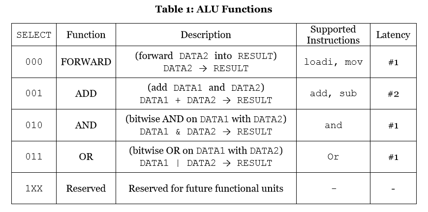
AluOp is the 3-bit signal which is generated by Opcode decoding. Operend1 and Operend2 will give the values to do the operation. ALURESULT will output the result.ZERO is the signal that shows whether the result is zero or not. It is used in beq instruction. Table 1 will give you the functions we have to implement.

The Verilog language we use latency only for simulation purposes. Now we will go and see coding.
          module alu(DATA1, DATA2, RESULT, SELECT,ZERO);
            //initializing the inputs and outputs
            input [7:0] DATA1;
            input [7:0] DATA2;
            input [2:0] SELECT;
            output [7:0] RESULT;
            output ZERO;                      reg [7:0] RESULT;
            reg ZERO;
            reg [7:0] RshiftResult;          barrelShifter myRightLogicalShifter(DATA1,DATA2[7:5],RshiftResult);
            //creating the always block which runs whenever a input is changed
            always @(DATA1,DATA2,SELECT)
            begin
            //selecting based on the SELECT input using s switch case
            case(SELECT)
            3'b000:
            #1 RESULT = DATA2; //Forward function
            3'b001:
            #2 RESULT = DATA1 + DATA2; //Add and Sub function
            3'b010:
            #1 RESULT = DATA1 & DATA2; //AND and Sub function
            3'b011:
            #1 RESULT = DATA1 | DATA2; //OR and Sub function
            //setting 1XX selection inputs.As there are reserved for future references it doesn't matter
            //for the time being the output was set to 0 when the select is 1XX
            3'b100:
            RESULT = RshiftResult;
            3'b101:
            RESULT = 8'b00000000;
            3'b110:
            RESULT = 8'b00000000;
            3'b111:
            RESULT = 8'b00000000;
            endcase
            end
            // creating the ZERO bit using the alu result
            //modified part
            always@(RESULT)
            begin
            ZERO = RESULT[0]~|RESULT[1]~|RESULT[2]~|RESULT[3]~|RESULT[4]~|RESULT[5]~|RESULT[6]~|RESULT[7];
            end
endmodule
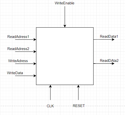
Then we will discuss the register File. In this case, we create a register module with eight 8-bit registers. This is the structure of the register module

We got 6 inputs and 2 outputs. We do register to write in the positive edge of the CLK signal. But reading is done asynchronously. We have a WriteEnable control signal to chose between write or don't write in every positive edge. ReadAdress signals give the registers which we should read.WriteAdress gives the register which we should write data.
We can implement it in Verilog like this.
module reg_file(IN, OUT1, OUT2, INADDRESS, OUT1ADDRESS, OUT2ADDRESS, WRITE, CLK, RESET) ;
//Initalizing inputs
input [2:0] INADDRESS;
input [2:0] OUT1ADDRESS;
input [2:0] OUT2ADDRESS;
input WRITE;
input CLK;
input RESET;
input [7:0] IN;
//initializing outputs
output [7:0] OUT1;
output [7:0] OUT2;
//initializing register variables integer i;
//creating the register array
reg [7:0] regFile [0:7];
//resetting the registers if the reset is 1 as a level triggered input
always@(*)
if (RESET == 1) begin
#2
for (i = 0; i < 8; i = i + 1)
begin
regFile [i] = 8'b00000000 ;
endend
//this always block runs of the positive edge of the clock and write to the register if write is ennable
always@(posedge CLK)
begin
if(WRITE == 1'b1 && RESET == 1'b0) begin
#2 regFile [INADDRESS] = IN; //this includes the write reg delay
//$monitor($time," %b",regFile [INADDRESS]);
end
end//this is for reading the inputs from the registers
endmodule
//this part was modified after the lab 5 part 3 submission
assign #2 OUT1 = regFile[OUT1ADDRESS];
assign #2 OUT2 = regFile[OUT2ADDRESS];
Now we have seen the design of a simple alu and register file which is implemented by Verilog. To build the processor we also need a Control unit and datapath. In the next part, I will show you how to implement those and how to build a testbench to run over Verilog code.
So good luck everyone. We will meet with part 2.
Part2 is now uploaded.
Thank You!
Feel like you're about to jump into a rabbit-hole of reading these incredible articles?
Don't worry, we feel the same way.
Not only can you jump into the rabbit hole with us, but we've got more than enough articles that'll help you jump out ;)
For some of the best ideas on Medium from the youngest minds of the generation, visit students x students.
How to Design a Microprocessor Using Verilog
Source: https://studentsxstudents.com/simple-8-bit-processor-design-and-verilog-implementation-part-1-8735fac284b
0 Response to "How to Design a Microprocessor Using Verilog"
Mag-post ng isang Komento